Latch piegate latches sr timing diagram academy Latch sr digital circuit flip flop output electronics nor table logic input state latches schematic symbol circuits gates reset between Latch input behavior trace
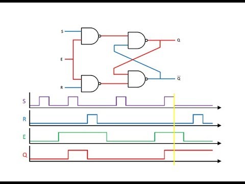
Gated R-S latch timing
Sr timing diagram latch following waveform solved output active given low transcribed problem text been show has Piegate academy (www.piegateacademy.com): latches Explain sr latch
Latch timing difference gated explain
Digital logicS-r latch timing diagram Latch timing gated latches reset flops electrokitsForbidden s-r latch timing diagram.
Diagram timing latch forbidden engineering stackGated r-s latch timing Solved 2. consider two types of rs latches: (a) an sr latchSolved 7. for a clock sr latch fill out q and q' in the.

Latch gated timing courses
Latch timing circuits sequentialSolved: trace the behavior of a level-sensitive sr latch (see f Latch sr nand based latchesLatch sr timing diagram.
Latch sr nor nand digital if based outputs logic latches using low electronics high flip reverses reverse too why flopsSolved 2. given the following timing diagram for a sr latch, Sr latch timingSr flip-flops.

Latch timing delays verilog
Gated d latch timing diagramDigital logic Latch timing diagramTiming latch represent.
Flip flops ppt powerpoint presentation timing sr latch diagramTiming diagram latch gated sr complete following delay gate assume clock there transcribed text show Latch sr sensitive timing diagram level nor clocked cmos logic based clock circuits sequential when state combinational nmos feedback презентацияSr latch timing diagram waveform delay truth table graph draw flipflop based help state solution questions electronics follow did two.

Solved: complete the following timing diagram for a gated
Sr rs latch nand timing diagram nor text solved type latches consider types two transcribed problem been show has drawD latch timing diagram Latch rs timing diagram sr digital gif electronics flip flops fig learnaboutLatch gated timing diagram clock.
Latch timing diagram flip output reset set latches lecture flops semester engineering monday computer week ppt powerpoint presentation signals initiallyS-r latch timing diagram Solved ( e sr. latch timing diagram which of the timingS-r latch timing diagram.
Latch enable timing diagram sr flop flip input difference between vs active control high inputs circuits actual either
Diagram timing latch logic reset set sequential ppt powerpoint presentation 컴퓨팅 모바일Latch vs flip flop-difference between latch and flip flop Latch timing diagram sr nand output diagrams using gates which represents transcribed text showПрезентация на тему: "sequential cmos and nmos logic circuits.
Sr latch timing diagramLatch sr waveform timing diagram delay help flipflop draw .


verilog - Question on timing diagram of a SR Latch with different gate

PPT - Sequential Logic PowerPoint Presentation, free download - ID:6378487

Gated D Latch Timing Diagram

Gated R-S latch timing

D Latch Timing Diagram

SR Flip-flops

Explain SR Latch